Fundamentals of piezoelectric ceramics
Piezoelectric materials
A piezoelectric material ((a) in the figure below) generates a charge when put under pressure ((b) & (c)). On the other hand, it will show a change in volume when an electrical field is applied. It can be used as a material for transforming electrical energy into mechanical energy and vice versa. Furthermore, applying an AC voltage to the material will cause it to vibrate, and thus generate mechanical waves with the same frequency as the electrical voltage. Similarly, if a mechanical vibration is applied, then a charge of proportional size and same frequency will be generated.
Piezoelectric activity was first discovered in single crystals by J and P Curie in 1880. Many years later, in 1946, it was discovered that barium titanate ceramics could be made piezoelectric by the application of an electrical field. This led to the further discovery of piezoceramics and the lead zirconate titanate-family, PZT. With its increased sensitivity and higher operating temperature, PZT soon replaced barium titanate in many existing devices and is still the most widely used piezoceramic today. The ceramic materials have several advantages over single crystals, including ease of fabrication in a variety of shapes and sizes and up to hundreds of times higher sensitivity. In contrast, single crystals must be cut along certain crystallographic directions, limiting the possible geometrical shapes.
Piezoceramics
Piezoelectric ceramics are, after firing, composed of small grains (crystallites), each containing domains in which the electric dipoles are aligned. These grains and domains are randomly oriented so the net electric dipole is 0, i.e. the ceramics do not exhibit piezoelectric properties. The application of a sufficiently strong D.C field will orient the domains in the field direction, as nearly as the orientation of the crystal axes allows. This ability to change the orientation of the domains and achieve a net polarization is called ferroelectricity. A remnant polarization can be created in ferroelectric ceramics by polarization. After the poling process is complete, a voltage causes expansion along the poling axis and contraction perpendicular to the poling axis. Compressive or tensile forces applied to the ceramic element will generate a voltage.
Definitions
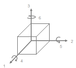
In piezoelectric ceramics superscripts and subscripts indicating direction are added to the symbols because material characteristics depend on the direction of the applied field, displacement, stress and strain. The direction of polarization is generally designated as the z-axis of an orthogonal crystallographic system. The axes x, y and z are respectively represented as 1, 2 and 3 directions and the axes shearing around these axes are represented as 4, 5 and 6. This is shown schematically on the next page. The various piezoelectric material constants are generally expressed with subscripts using this notation. Planar modes are sometimes expressed with a subscript ‘p’ and the thickness mode with a subscript ‘t’. The first subscript gives the direction of the electrical field associated with the voltage applied or the charge produced. The second gives the direction of mechanical stressor strain. Superscripts indicate a constant mechanical or electrical boundary condition.
| Parameter |
Symbol |
Condition |
| Stress |
ơ |
Mechanically free |
| Field |
E |
Electrical short circuit |
| Displacement |
D |
Electrical open circuit |
| Strain |
S |
Mechanically clamped |
Curie temperature
The crystal structure of a material changes at the Curie temperature, Tc, from piezoelectric (non-symmetrical) to a non-piezoelectric (symmetrical) form. This change in phase is accompanied by a peak in the dielectric constant and a complete loss of all piezoelectric properties.

 ENGLISH


